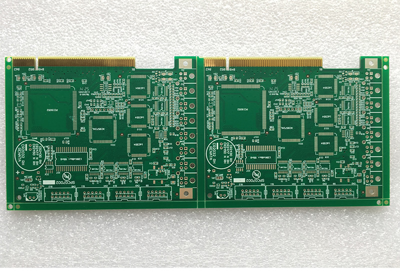
| Layers | 6 layers |
| Board thickness | 1.60MM |
| Material | FR4 tg170 |
| Copper thickness | 1/1/1/1/1/1 OZ(35um) |
| Surface Finish | ENIG Au Thickness 0.05um; Ni Thickness 3um |
| Min Hole(mm) | 0.203mm filled with resin |
| Min Line Width(mm) | 0.13mm |
| Min Line Space(mm) | 0.13mm |
| Solder Mask | Green |
| Legend Color | White |
| Mechanical processing | V-scoring, CNC Milling(routing) |
| Packing | Anti-static bag |
| E-test | Flying probe or Fixture |
| Acceptance standard | IPC-A-600H Class 2 |
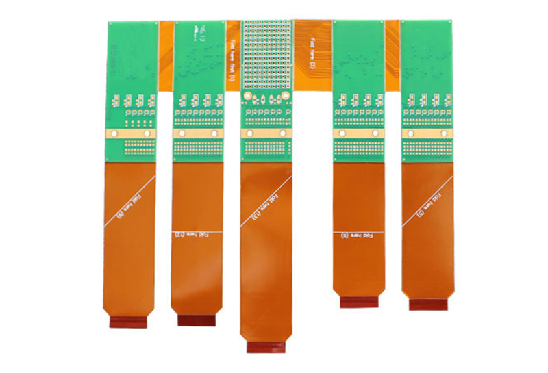
| Application | Automotive electronics |
| Components | Thickness | Tolerance | Weave type |
| Internal layers | 0,05mm | +/-10% | 106 |
| Internal layers | 0.10mm | +/-10% | 2116 |
| Internal layers | 0,13mm | +/-10% | 1504 |
| Internal layers | 0,15mm | +/-10% | 1501 |
| Internal layers | 0.20mm | +/-10% | 7628 |
| Internal layers | 0,25mm | +/-10% | 2 x 1504 |
| Internal layers | 0.30mm | +/-10% | 2 x 1501 |
| Internal layers | 0.36mm | +/-10% | 2 x 7628 |
| Internal layers | 0,41mm | +/-10% | 2 x 7628 |
| Internal layers | 0,51mm | +/-10% | 3 x 7628/2116 |
| Internal layers | 0,61mm | +/-10% | 3 x 7628 |
| Internal layers | 0.71mm | +/-10% | 4 x 7628 |
| Internal layers | 0,80mm | +/-10% | 4 x 7628/1080 |
| Internal layers | 1,0mm | +/-10% | 5 x7628/2116 |
| Internal layers | 1,2mm | +/-10% | 6 x7628/2116 |
| Internal layers | 1,55mm | +/-10% | 8 x7628 |
| Prepregs | 0.058mm* | Depends on layout | 106 |
| Prepregs | 0.084mm* | Depends on layout | 1080 |
| Prepregs | 0.112mm* | Depends on layout | 2116 |
| Prepregs | 0.205mm* | Depends on layout | 7628 |

Q&A How To Test Hole Wall Tensile And Related Specifications
How to test hole wall tensile and related specifications? Hole wall pull away the causes and solutions?
Hole wall pull test was applied previously for through-hole parts to meet assembling requirements. General test is to solder a wire onto the pcb board through holes and then measure the pull out value by the tension meter. Accords to the experiences, general values are very high, which makes almost no problems in application. Product specifications varies according to different requirements, it is recommended referring to IPC related specifications.
Hole wall separation problem is the issue of poor adhesion, which generally caused by two common reasons, first one is the grip of poor desmear (Desmear) makes the tension not enough. The other is the electroless copper plating process or directly gold plated, For example: the growth of thick, bulky stack will result in poor adhesion. Of course there are other potential factors may effect such problem, however these two factors are the most common problems. There two disadvantages of hole wall separation, the first one of course is a test operating environment too harsh or strict, will result in a pcb board can not withstand physical stress so that it is separated. If this problem is difficult to solve, maybe you have to change the laminate material to meet improvement.
If it is not the above problem, it is mostly due to the poor adhesion between the hole copper and the hole wall. The possible reasons for this part include insufficient roughening of the hole wall, excessive thickness of chemical copper, and interface defects caused by poor chemical copper process treatment. These are all is a possible reason. Of course, if the drilling quality is poor, the shape variation of the hole wall may also cause such problems. As for the most basic work to solve these problems, it should be to first confirm the root cause and then deal with the source of the cause before it can be completely solved.